PYNQ Tutorial 3: Custom IP core and the Block Design
This is the third part of the PYNQ tutorial series. This article is about the usage of custom IP cores and block designs. Actually these are board independent: they are just Vivado tricks and Verilog, nothing is specific to PYNQ, we don’t even need to run synthesis.
I didn’t found any material about these subjects in our school’s related courses and had a hard time dealing with these, so I decide to make a tutorial.
You may need basic knowledge about Vivado design procedure(like create source code file, run simulation and use IP core) to understand this.
Notice:
Projects and source code used in this and the following tutorials are available at Github here: github.com/regymm/PYNQ-Tutorial-Material.
Aiming at simple-to-use, these Vivado projects are directly added to git, instead of using better tcl methods. You can directly open the .xpr project files in Vivado and run simulations & other things.
Create a Custom IP Core
Create and package a new IP is just turning your existing module into a library which can be used by other Verilog programs, which is actually very easy.
I have a small module which delay the input signal whose width may vary for a clock cycle, let’s use this as example:
`timescale 1ns / 1ps

module delaypass #(parameter W = 32)
(
input clk,
input [W-1:0]din,
output reg [W-1:0]dout
);
always @ (posedge clk) begin
    dout <= din;
end
endmodule
Two input, one output, one configurable parameter. And of course, having a Vivado project contains this as it’s top module(here called delaypass). Quite simple.
What to do next?
In the top menu bar, choose Tools->Create and Package New IP....
Hit next, then the default option Package your current project(Just as the description, we are going to use the whole project as a new IP. We may encounter the AXI4 Peripheral in next tutorial but for now just ignore that) and next again.
Then choose the location. It’s easy to mess up here(relax, this kind of mess up often doesn’t matter), and to choose the location inside the project seems to be a plausible way for me. Here I just choose delaypass the project root directory. If you are doing this again and again you’ll need to hit Overwrite in the prompt. It doesn’t matter. Then hit Finish.
You’ll see a packager like this:
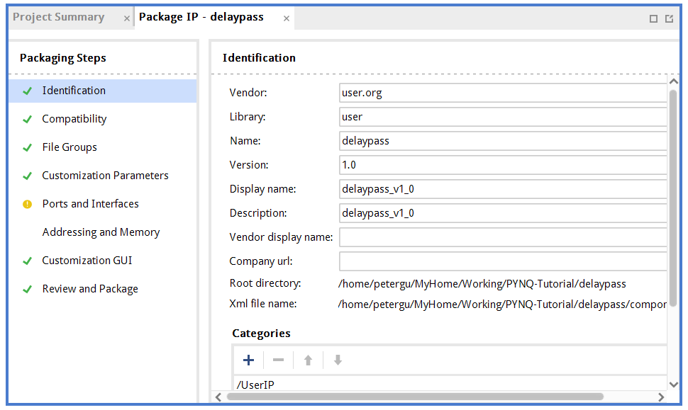
,where you can specify name and version of the IP. Then jump to the Review and Package tab and hit Package at the bottom. You’ll see the IP created in the delaypass directory: there’s a component.xml file containing the IP info, you can have a check.
After that an Edit Packaged IP option will occur on the left side, just below IP Catalog, hit it and the packager will show up again and you can modify your IP.
But of course, you can also redo the Create and Package New IP... process and overwrite instead, which, for me, seems to be able to avoid many frustrating problems, and actually save my time.
There are many more tricks and traps about this process, some are shown below and more are up to you to find. Buy anyway, packaging IP is much easier than(and should be, if you’ve got used to it) writing your project code, isn’t it?
Use the Core
Let’s try to use our packaged IP core in another project: here the ip_test_and_bd.
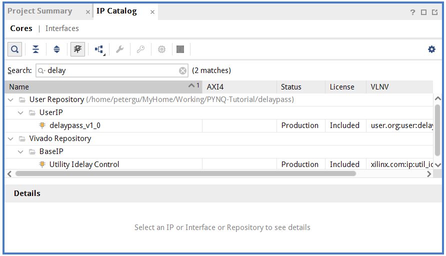
Of course Vivado won’t know your IP core which is now lying in a corner of your disk, so first go to PROJECT MANAGER->Settings->IP->Repository, and add the delaypass directory. You’ll see the friendly notification that 1 IP is added.
Then go to IP Catalog the same as before, search for delaypass, and our IP appears:
Choose it and customize(though there are not too much to customize), then OK as normal:
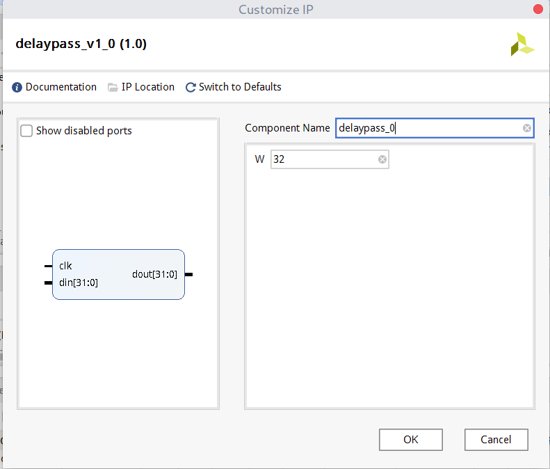
You see on the left graph input and output ports are shown, and on the right side is customization, just like in existing ones like this adder(though the adder is more complex):

Then the IP core is in your project, just use it like others ones! For example, try the simulation source:
`timescale 1ns / 1ps

module delaypass_test();

reg clk = 0;
always @(*) #10 clk <= ~clk;

reg [3:0]din;
wire [3:0] dout;

delaypass_0 #(.W(4)) delaypass_inst
(
    .clk(clk),
    .din(din),
    .dout(dout)
);

initial begin
#2
din = 4'b0000;
#20
din = 4'b0100;
#20
din = 4'b1100;
#20
din = 4'b0110;
#20
din = 4'b1101;
#60
$stop;
end
endmodule
Hoping that IP cores are no longer mysterious to you any more!
Use a Block Design
If you look up some ZYNQ tutorial, then probably you’ve seen those eyesore “block designs”, and you cannot circumvent them as far as I know. But after reading this you may find them acceptable.
Block designs are to make things easier: Imagine you need to wire up a lot of IP cores, like adders multipliers, and our own delaypass, there are more than ten of these. So you’ll feel very annoyed if you need to write these in Verilog: all these IPs and all connecting wires, to write by hand!
Then you’ll image what things will be like if you can just maintain these IPs and wires in a graph, and do connections by simply dragging mouse: this is what the block design will do for you. (If you’ve used LabVIEW you’ll be quite familiar with this)
And after that, you can use the block design the same as a normal module: which, if to be written by your hand, may take an infinite amount of time.
Now get down to the point.
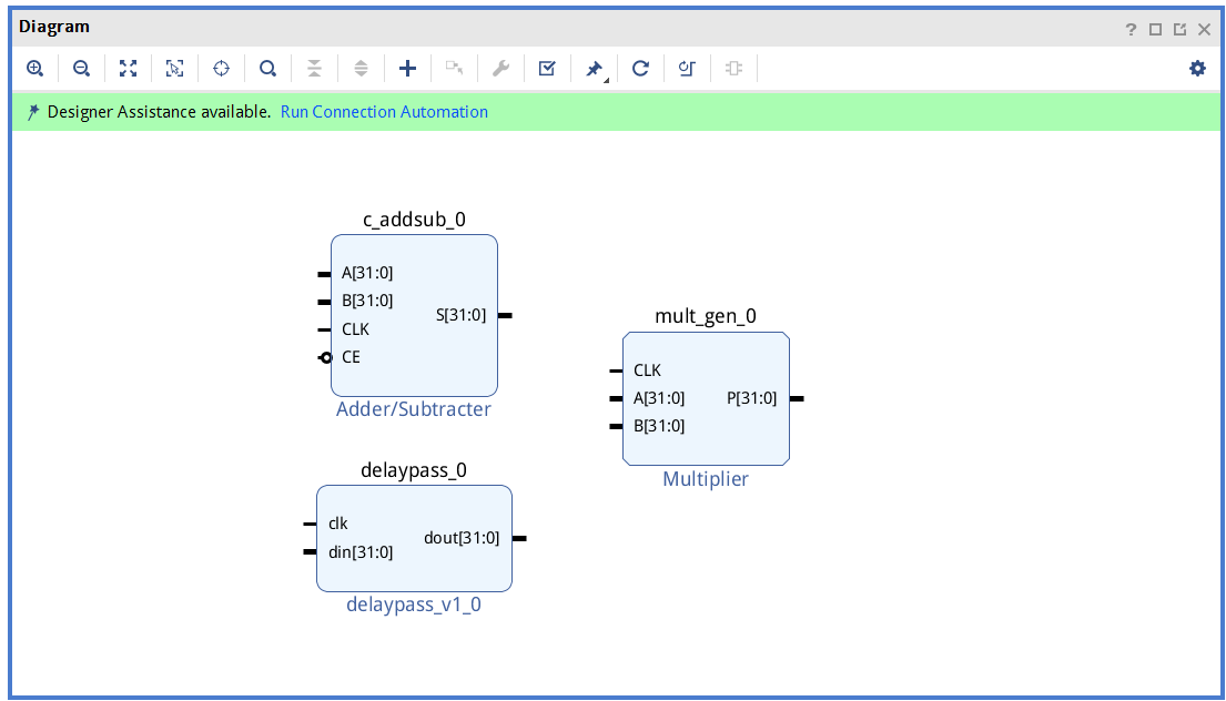
Click Create Block Design on the left panel. OK. And you get an empty diagram. Right click and Add IP..., you can try to add a few IP cores, like an adder(1 cycle delay), a multiplexer(1 cycle delay), and a delaypass, and customize them. For example, turn all width to 32. Drag to place them like this:
Use mouse to drag wire:
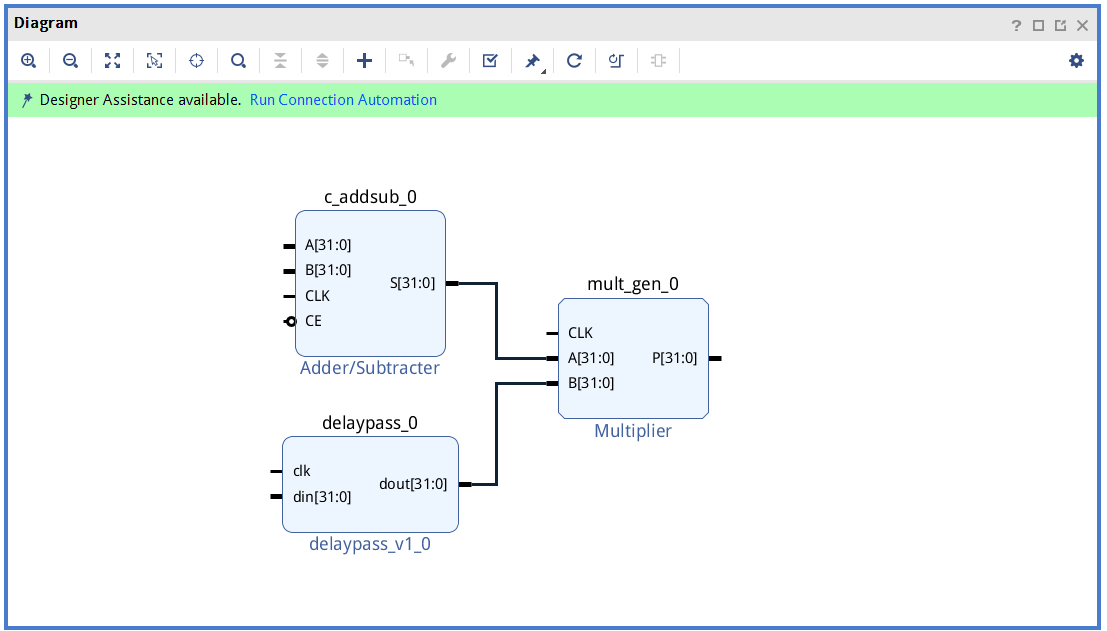
Right click at blank to add some input and output: A B C as input, clk as input, O as output. Let the clk to be 100Mhz is OK.
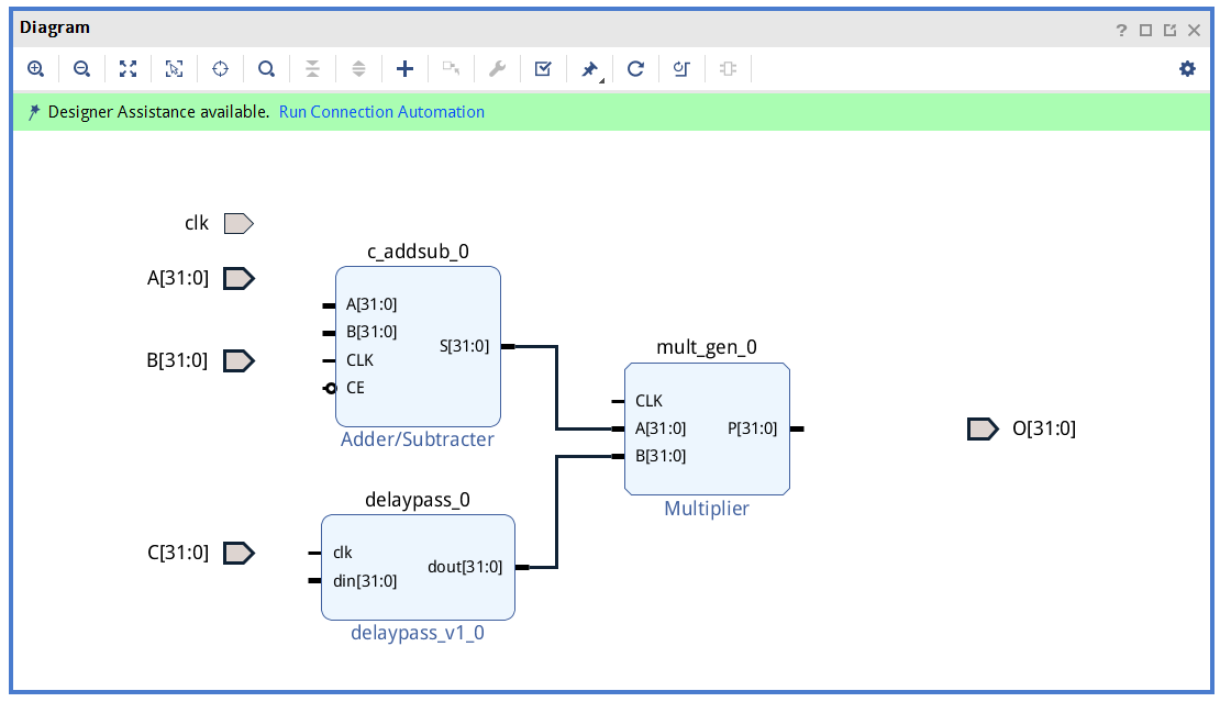
Now you may have figured out what we are doing: calculate O=(A+B)*C with 2 cycle delay, with pipeline.
Then connect the wires. You can use the “Connection Automation” to automatically connect some parts(like clocks): now it’s not necessary, but if the block design is an order of magnitude larger, you’ll find this function extremely useful.
The finished block design:
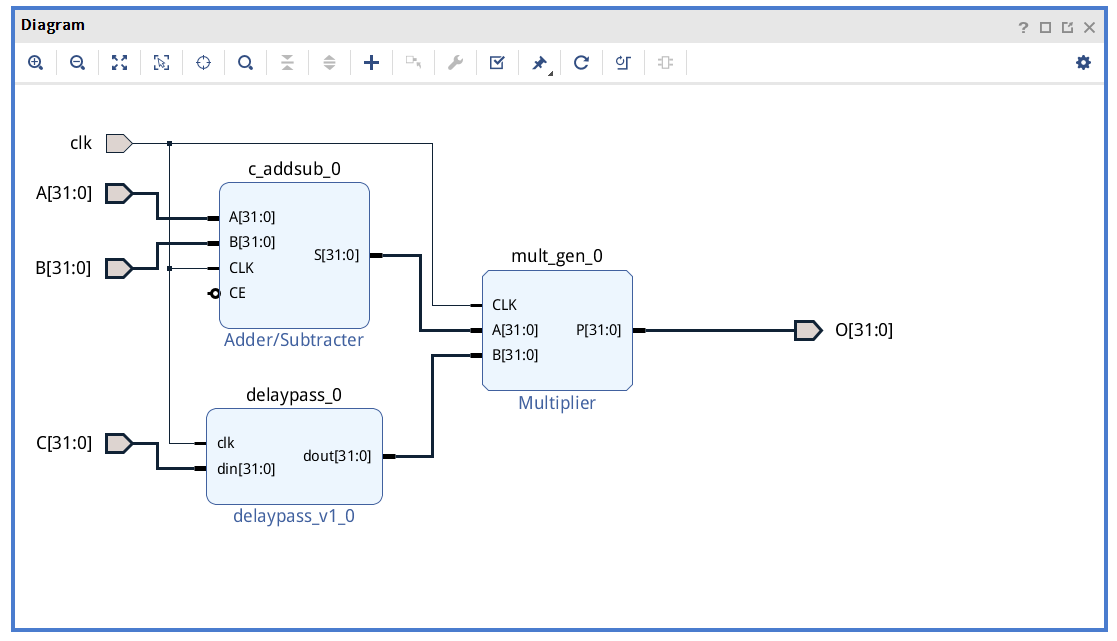
You can choose to auto-clean it using the “Regenerate Layout”(the reboot-like symbol on top), but just like in LabVIEW, if the diagram is small you can just lazily write a messed-up panel then auto-clean it, while when the diagram is big(e.g. fills the entire monitor screen), you’ll be completely lost after auto-clean and unavoidably have to undo it.
Now let’s add another simulation file and have a try:
`timescale 1ns / 1ps

module bdtest();

reg clk = 0;
always @(*) #10 clk <= ~clk;

reg [31:0]A = 0;
reg [31:0]B = 0;
reg [31:0]C = 0;
wire [31:0]O;

design_1 design_1_inst
(
    .clk(clk),
    .A(A),
    .B(B),
    .C(C),
    .O(O)
);

initial begin
#2
A = 1;
B = 1;
C = 1;
#20
A = 2;
B = 2;
C = 2;
#20
A = 4;
B = 9;
C = 10;
#60
$stop;
end
endmodule
Fire up a simulation and change radix to decimal:
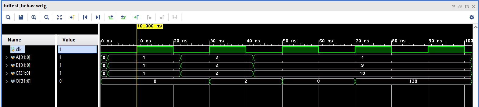
You see, we get the result O=(A+B)*C after two cycles, and because of the pipeline we can get one result per each cycle.
What’s Next
In the next tutorial let’s go back to PYNQ. We’ll do a simple and painless PS/PL communication.
It’s the end. At least for now.
 This work is licensed under the Creative Commons BY-SA 4.0 International License, if not explicitly specified.