A Failed Attempt of Chip Making - Writeup
In the first semester of the third year, their’s a course called “research-oriented physics experiment” in which we form groups and choose experimental subjects from solar cells making to quantum dot preparation. And somehow, I came up an idea, why not try making some chips? A quick search gave Jeri Ellsworth and Sam Zeloof’s Youtube video – less than half an hour’s tutorial and working transistors? Not bad! I don’t know what my teammates thought but for me it’s especially like diving into the deepest level of the Age of Information.
First we wanted to follow the processes of these two person – silicon based transistors from doped wafers. But of course, the truth was nothing worked as expected: the oven was not the open ones which we could put in and take out samples at any time, our hydrophobic wafer didn’t like the boric solution, and hydrofluoric acid was making us nervous especially in the crowded public lab.
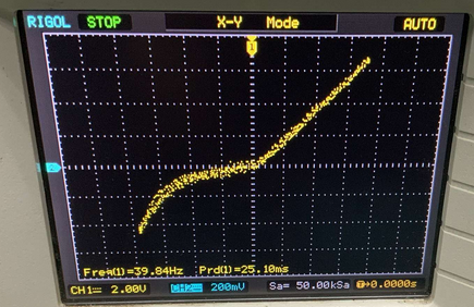
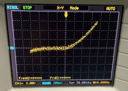
Anyway here’s what we got: 1000 degree C burnt silicon pieces, some P-N junctions and their voltage-current waveforms(by a custom breadboard curve tracer):
- Sample 1
- Sample 2
- Sample 3
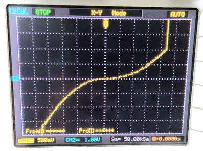
Some looks like real junction, while others like multiple unknown things sticked together. They are all garbage compared with the commercial(real) diode:

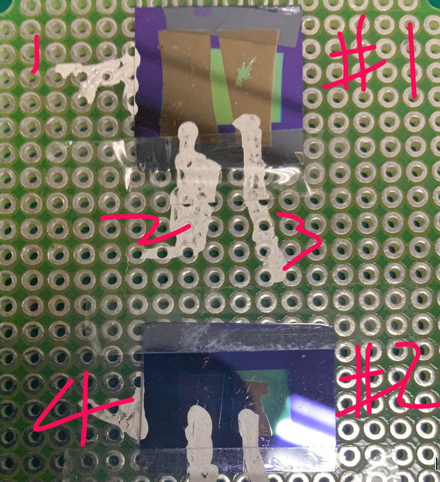
Then we thought we should utilize the lab’s modern equipments better: magnetic sputtering and evaporation coating. And we turned to zinc oxide which seemed to be more common for sputtering. Papers were read, experiments were performed(inefficiently), but in this unfamiliar field, we can’t even explain our own experiment results. For example what’s going on when junctions are generated when sputtering ZnO onto silicon wafer with >300nm oxidation layer? How much voltage can it handle(As I saw sparkles during testing)?
All we got was a better but less-understood junction – transistor are just too far away!
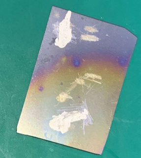
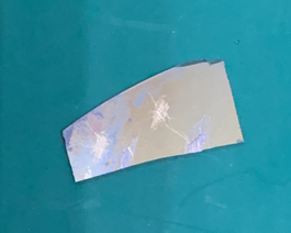
The purple is oxidation layer, middle green is ZnO layer, and brown is aluminum(should be silver color but hey!).
Waveform between 1 and 3:
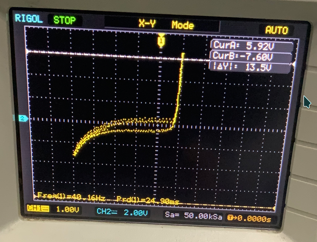
The hysteresis seemed to indicate a large capacitance, though we don’t know why. I scratched off the Al layer, the junction still exists, only with bigger resistance.
Recently I came across this on Sam Zeloof’s Twitter(not sure if others are allowed to re-post this):
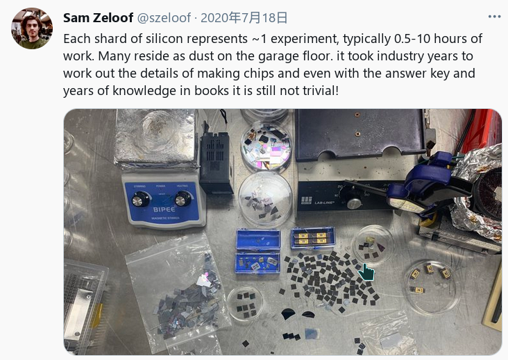
And now I know three months are far less time than required for something like this.
During that period, I read dozens of research papers related, on physics or chemical journals. I never felt so motivated to read papers before. But what I was doing is not research isn’t it? It’s just DIY and reinventing the wheel with extra steps.
However, this dream won’t end.
 This work is licensed under the Creative Commons BY-SA 4.0 International License, if not explicitly specified.