From RTL and No-RTL to GDS in 3 Weeks
Ever used xschem?
Pressing button on other people’s design only.
Ever used klayout?
Installation & importing library.
First time tapeout?
Second.
First time analog?
You bet.
Toolchains development?
Finger crossed.
Aug 22
Forked repo
Downloaded vhdx image from Ishi-kai and converted to Docker image
Locally run example signoff flow in another Docker image from GitHub CI flow
Aug 23
Staring at inverter and kinda understood how it works, what are the layers mean.
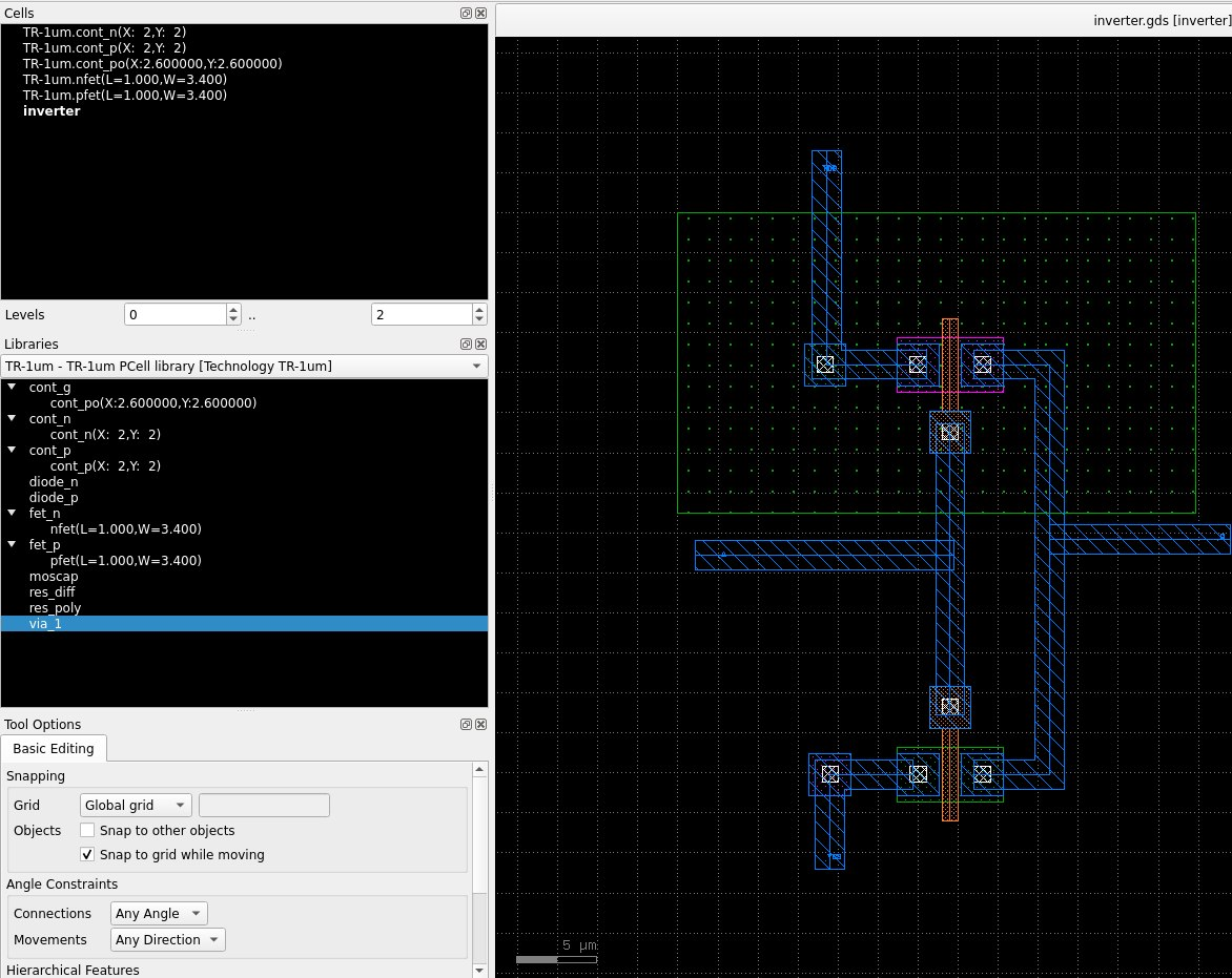
Get idea about size of standard cells and total size available.
Understand the flow – what exactly xschem and klayout does, comparing with PCB, how to make sure schematics and layout matches.
Aug 24
Learned working principle of TDC
Idea about the TDC which I never got time to do on FPGA.
Idea about photonic devices
3-week timeline sanity check
Digital flow possibility (no)
Aug 25
Get to know ring oscillator and it’s one of the simple demos available
Understand why stdcell inverter is “huge”.
Understand what xschem can (gate-level simulation, inverter up/fall time) and can’t (for this, parasitic things, line delay) do.
Get to know PEX is not available but kinda not necessary here.
Learn what LVS does, quickly got that it’s really important!
Possibility about hierarchical schematics / sym / LVS – it’s certainly possible and recommended.
Based on Ishi-kai tutorials, get a inverter xschem simulation.
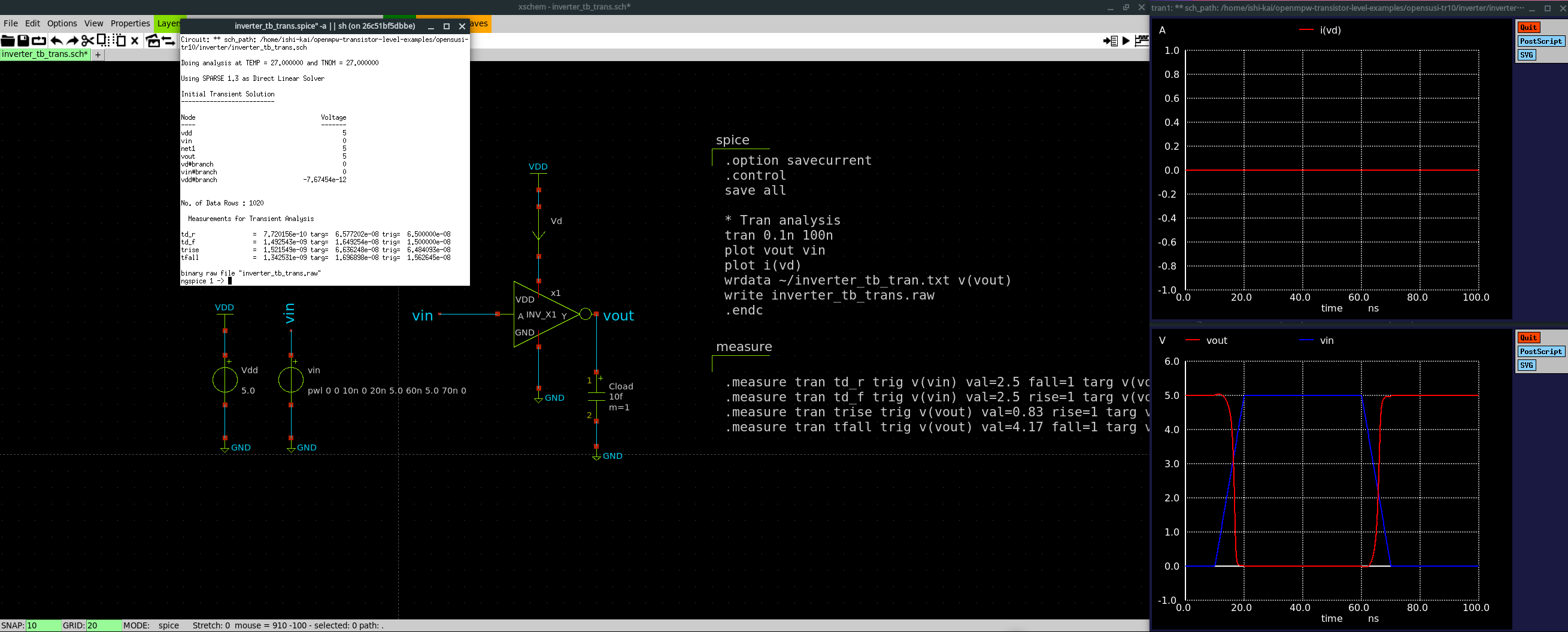
Then comes ring oscillator (RO) – simulated frequency ~150 MHz for 5 stages.
RO with a NAND gate for enable pin
By adding another MOS, got a voltage-controlled oscillator simulation.
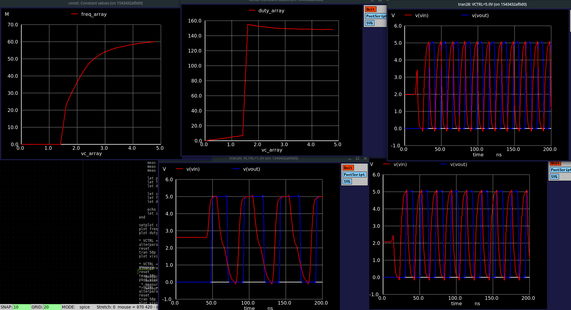
Learning to write some spice.
Got into tedious lab_pin, io_pin name conflict problems.
Understand INV/BUF x1/x8/x16 differences
Wondering where to start klayout, if there’s a schematics-to-layout tool (no)
Connecting metal with an array of stdcell inverters.
Understand DRC errors about WN
Understand how MOS is a 4-port device, whether VSS/VDD is well connected, substrates, and how LVS handles this
Fight with GND/VCC LVS
Talked with team member about PDK histories.
I guess this is the day the tapeout decision was made.
Aug 26
Evaluate how much space is required, how many taps is available for TDC
Think about input delay of TDC, just think.
Understand what structure the I/O pads have (big ESD MOS)
Programmable voltage in xschem
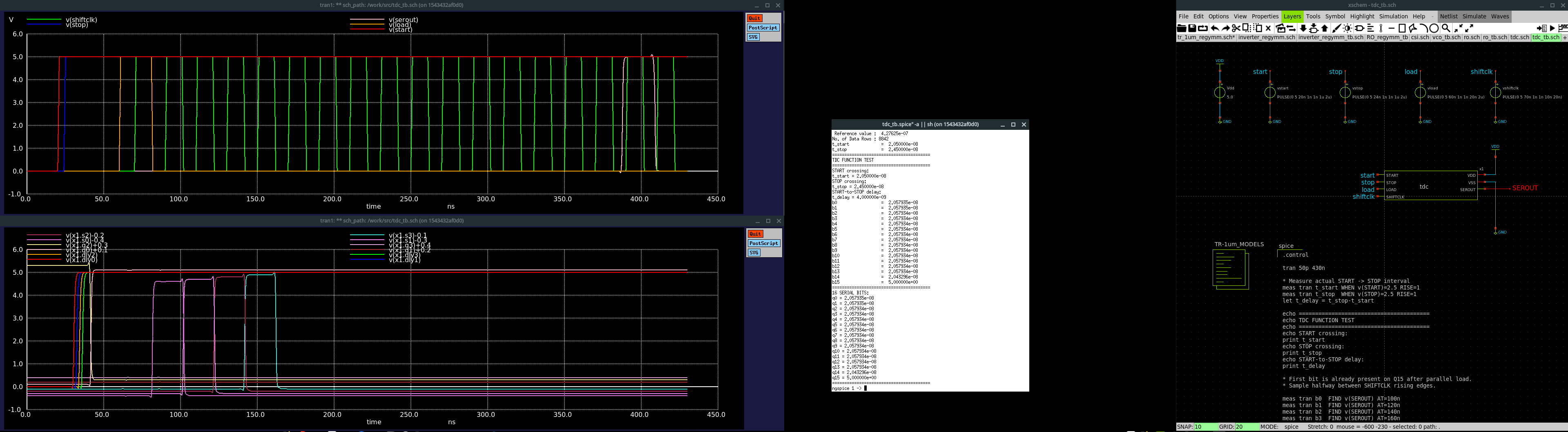
TDC schematics passing xschem simulation, got ~2 ns per tap
Awful problem about LVS and pin names on GDS, cells in GDS, moving lines and vias breaking cells
Aug 28
Pin name moving from M1 to TXM1
Brainstorm about photonic devices
Sep 2
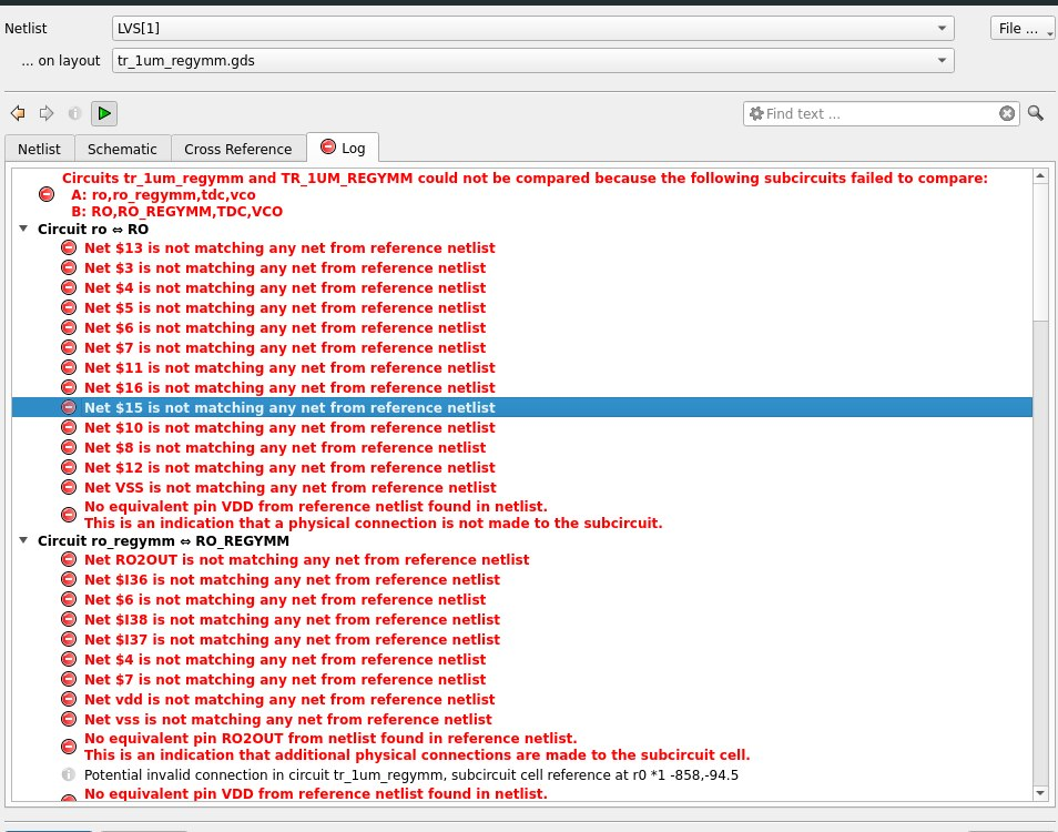
LVS error when combining module into one, each module passes individually but the top module won’t
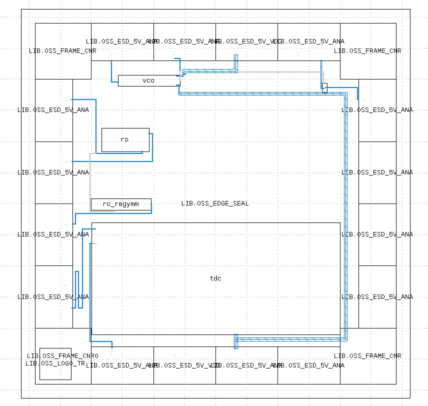
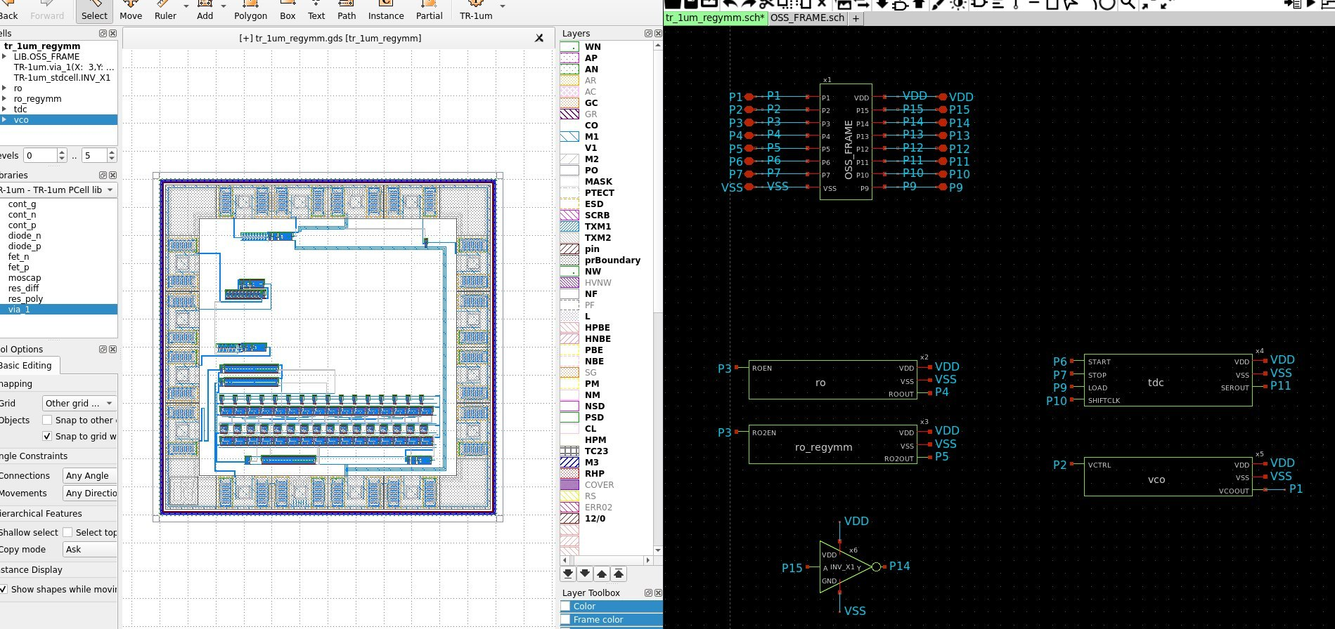
Friend’s working on a digital flow.
Sep 3
VSS/VDD metal wire width, from senior advice.
The LVS error was due to different cell names, solved by replacing all cells manually in child GDS module – not fundamental but works.
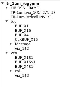
Placing a (photo)diode and get to know how it works, how the WN contact affects LVS – LVS really checks a lot of things!
Size of the diode, and why RC makes larger ones slow
Sep 4
Got to know friend’s librelane flow is close to signoff
Sep 6
DRC & GDS & GitHub CI passing with manually-placed designs (INV + RO + custom RO + VCO + TDC + Photodiode)
What to do with 1 left pin. Pressure-sensitive or microphone? Impossible.
Sep 9
Really thinking about the digital flow, targetting 20% chip space for a UART TX
Continue to analyze how much static characters can fit into the 20% chip space, various optimizations like all-capital characters and reuse counters. Even thought about a math formula to generate the characters – but no, same amount information is required anyways.
Sep 10
Really begin working on the librelane flow
Sep 11
Fixing librelane flow with upstream
Sep 12
Having RTL-GDS output, realized power problem are very different from FPGA!
Sep 13
Seems OK result
Sep 14
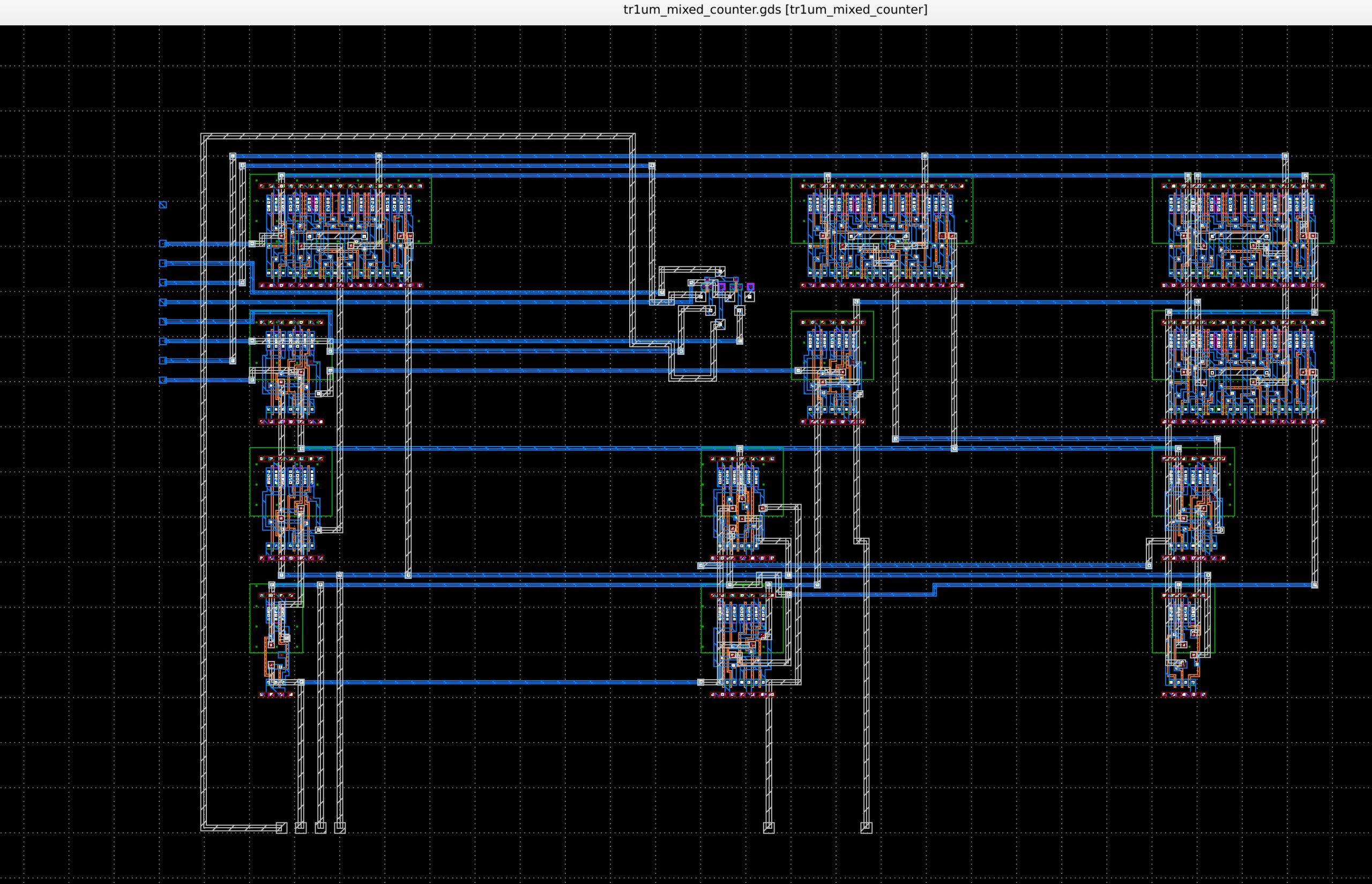
Only one counter is used to drive from char selection to baud counting – this requires a very weird input frequency! Think about where the clock input comes due to the limited pins.
DRC/LVS clean UART GDS, outputting 24 big characters. See how the N-well are connected altogether.
Sep 15
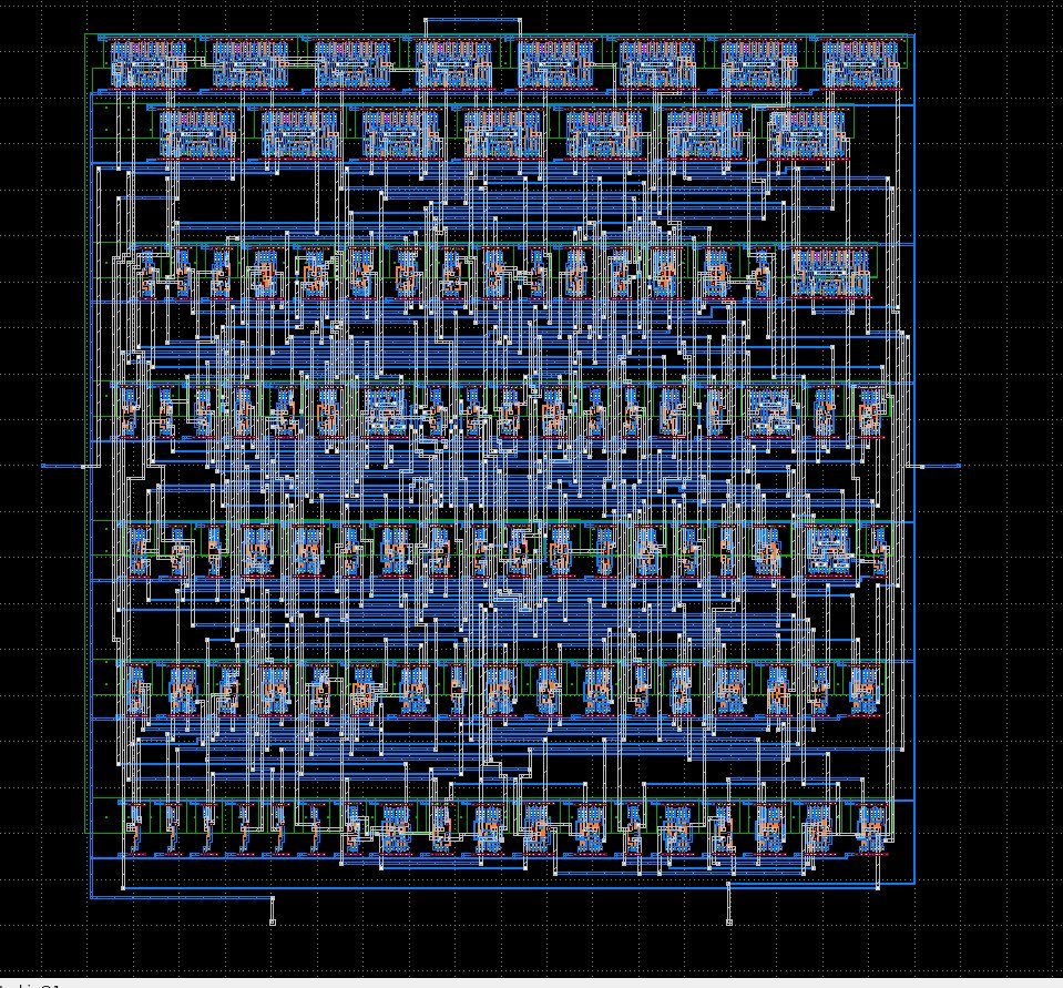
Lots of optimizations and more examples with librelane flow
UART netlist gate-level simulation, see hazards in the combinatorial output, but seems OK
50 MHz clock is suspicious but 5 MHz works
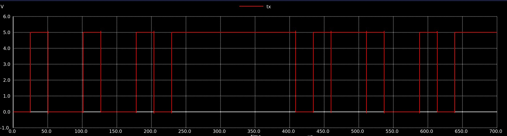
Evaluate the 50 MHz-level clock compared with previous RO frequency
Compare how 130 nm/55 nm scales the frequency
Understand Power Distribution network needs special care in ASIC
DRC/LVS works but foundry IP62 DRC have error, then fixed this
UART netlist/spice model updated
GDS Submission 1
Logo, image to GDS, submission 2
Slightly fancier online GDS viewer
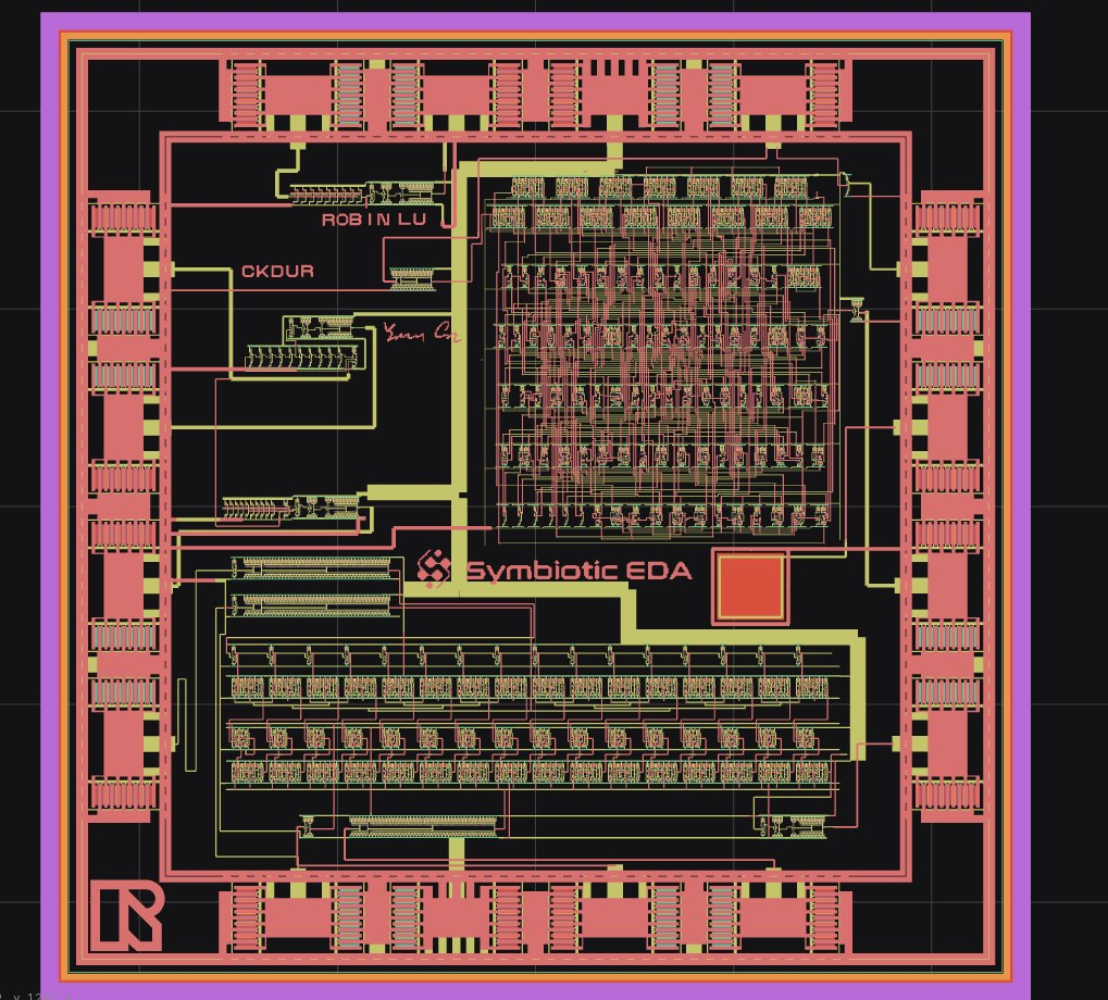
Pull Requested minor fix to https://github.com/kadomoto/picture-to-gds
Sep 16
Pull Requested to https://github.com/luyanna/TR-1um libreline flow upstream, including GitHub CI
 This work is licensed under the Creative Commons BY-SA 4.0 International License, if not explicitly specified.