How I managed to boot ZYNQ and load PL bitstream, w/o DDR, now w/o QSPI Flash
The Backstory
ZYNQ 7000 series are wonderful devices. What more can you wish for an embedded system than the ARM A9 (PS) + FPGA fabric (PL) combo?
It’s born a high device, the first time I came across it is when I first started FPGA development in undergraduate. The course (which I didn’t join) uses Nexys 4 DDR, but two of my friends one day showed up with a ZYBO, saying it’s “less expensive”. I remember them using the Xilinx SDK, booting from SD card with a file called BOOT.BIN, and pausing the CPU to debug. I don’t know the trick of pausing CPU even today, but when they returned to the dormitory in the morning with breakfast in hand I could guess it’s not an easy situation.
Two months passed, and when I’m thinking seriously about making my very own FPGA board, the very same friend advised me to consider ZYNQ, nothing but because of its unreal price. Since it’s my first 4-layer PCB and I just want the FPGA part, PS DDR’s off the table. He also offered to implement a PCIe stack if I dare to put it on the PCB – but after knowing the Xilinx 7-Series High-Range IOs’ speed limit and the rarity of external PCIe PHYs, that’s also off the table. Yes, we do have PCIe-to-UART bridge chips off-the-shelf, but that can barely be called interesting.
A little bit background: that’s late 2020 in China, we’re back to school and chip shortage is not a thing yet. EBAZ4205, the retired mining rig’s controller board, is at its ever-low price of 15 RMB per piece. Because of this, a ZYNQ 7010 chip, refurbished, costs just two cans of coke.
No DDR
Nearly every ZYNQ development board on sale has DDR, for obvious reasons, albeit the rare case also works. Back in 2014 the support is rather elusive and you need to keep the “Enable DDR” in Vivado. Later things becomes easier and it’s just patch a few lines of code and modify the linker script.
Now this Zynq 7000 Tips and Tricks entry is latest I can find. In case it disappears some day, I’ll briefly copy it here:
-
Deselect “Enable DDR” in Vivado, then export HW, launch SDK, new FSBL project as usual.
-
Remove (or disable by macro) this DDR init code in main.c in FSBL code
Status = DDRInitCheck(); if (Status == XST_FAILURE) { fsbl_printf(DEBUG_GENERAL,"DDR_INIT_FAIL \r\n"); /* Error Handling here */ OutputStatus(DDR_INIT_FAIL); /* * Calling FsblHookFallback instead of Fallback * since, devcfg driver is not yet initialized */ FsblHookFallback(); } -
Remove the DDR address check in image_mover.c
if ((PSPartitionFlag == 1) && (PartitionLoadAddr < DDR_START_ADDR)) { if ((PartitionLoadAddr == 0) && (!((SignedPartitionFlag == 1) || (EncryptedPartitionFlag == 1)))) { break; } else { fsbl_printf(DEBUG_GENERAL, "INVALID_LOAD_ADDRESS_FAIL\r\n"); OutputStatus(INVALID_LOAD_ADDRESS_FAIL); FsblFallback(); } } if (PSPartitionFlag && (PartitionLoadAddr > DDR_END_ADDR)) { fsbl_printf(DEBUG_GENERAL, "INVALID_LOAD_ADDRESS_FAIL\r\n"); OutputStatus(INVALID_LOAD_ADDRESS_FAIL); FsblFallback(); } -
The PartitionMove function in image_mover.c can be changed as the following:
but I found it’s not that necessary.
if ((PLPartitionFlag && !SignedPartitionFlag) || (!PLPartitionFlag && ((PartitionExecAddr != 0 && ((PartitionExecAddr < QSPI_FLASH_BASEADDR) || (PartitionExecAddr > QSPI_FLASH_HIGHADDR))) || ((PartitionLoadAddr >= 0xFFFF0000) && (PartitionExecAddr == 0)) || ((PartitionLoadAddr == 0x40000000) && (PartitionExecAddr == 0))))) { Status = PartitionMove(ImageStartAddress, HeaderPtr); if (Status != XST_SUCCESS) { fsbl_printf(DEBUG_GENERAL,"PARTITION_MOVE_FAIL\r\n"); OutputStatus(PARTITION_MOVE_FAIL); FsblFallback(); } } -
In the linker script, make sure all segments uses OCM memory space (and SPI Flash’s mapped memory), instead of DDR. Block RAMs in the PL can also be used once the bitstream (with correct AXI devices inside) are loaded, and ps7_post_config can configure them in FSBL.
It’s FSBL but you can just launch it from SDK to hardware as usual, same as a hello-world example. It will try booting from the real QSPI/SDCard and probably fail, but the initial parts can be checked.
I also learned the importance to have a real switchable boot options, instead of just tie the pins hard down to use QSPI/SDCard – in case you’ll need to program the QSPI from SDK, or load test code from JTAG and test something more than a hello world, the boot option will be checked by the SDK, only a real JTAG boot will help.
Shady potentials
In theory, the SDRAM or DDR3 on PL can also be used with the driver’s AXI interface hooked to PL, giving a few dozens of MBs or even Gbs, enough to run Linux. By this way, every single memory transaction from the ARM cores to Linux can be monitored, recorded, and tampered – giving a perfect embedded Linux verification or hacking platform?
Some fine partial reconfiguration setup may even allow bitstream being loaded on-the-fly without disrupting PS-to-memory transactions.
But I’ve never seen a single ZYNQ board with DDR on PL but not PS. So far. The reason is obvious enough, PS DDR on a Zynq 7000 can go to 667 MHz, DDR on Artix 7 fabric with -1 speed grade usually stops at 400 MHz. On UltraScale+, a 4GB PS DDR4 + 1GB PL DDR4 combo is very common, but on 7-series, the PL really doesn’t have too many IO pins to spare.
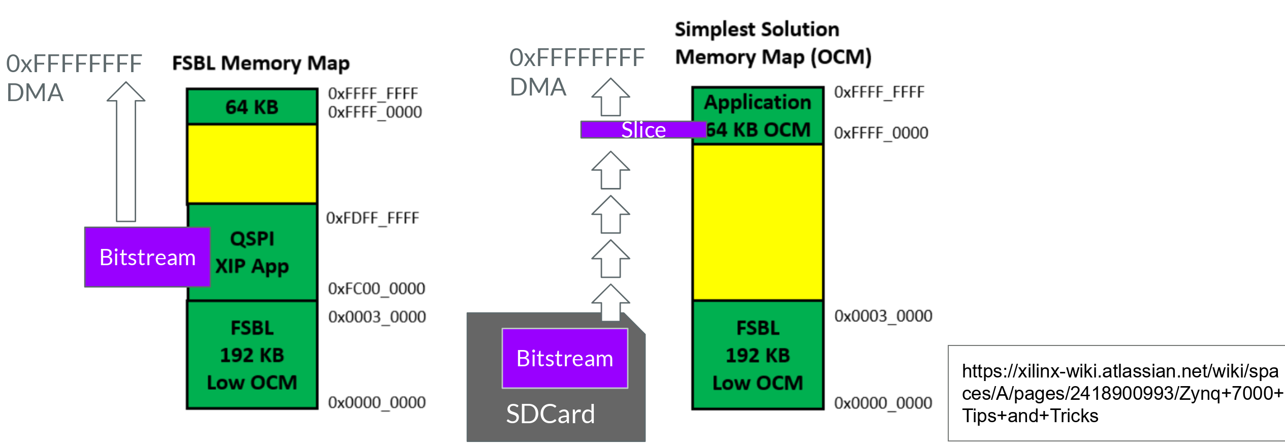
Do we need a continuous memory?
How is the bitstream loaded from the beginning? It’s done by the PCAP interface. In brief, the bitstream is put into a serial memory region, and a DMA request is sent with destination address 0xFFFFFFFF, which loads the bitstream: here.
One major task in No-DDR SD boot is that the bitstream in QSPI Flash is memory-mapped, and can be used for executin-in-place (XIP). This allows a single DMA requires to be issued to load the whole bitstream, with a size larger than the OCM, into the PL.
Here’s the memory layout of Zynq bootstage w/o DDR, and certainly the only large-enough block to hold the bitstream is the QSPI.
No one had done it, but it works
Previously, I had some discussion in an online group. I even said “the DMA might be done slowly”, but the 0xFFFFFFFF write address is too counter intuitive to overthink – it’s natural to think that a write to such an symbolic address shouldn’t be messed up with. I thought connecting JTAG back to EMIO and bit-bang in FSBL would be the only choice left.
However, recently, when I really tuned the FSBL PCAP code, and tried spliting the DMA request into two, then into one hunderd, miracle appears and bitstream can load as usual! This means one single big memory region is not required, and we can read bitstream from SD card, and DMA it chunk by chunk into the PL fabric – with growing Source Address, but the same straight-F Destination Address. Guessed it may work, didn’t expect it really does! The speed penalty is relatively small (<0.5s difference for a Zynq 7020’s uncompressed bitstream).
In my slides, this process is described like this:
This works, together with the OpenXC7 toolchain that supports now Zynq 7030/7035/7045/7100’s PL fabric as well, has been presented on FOSDEM 2025. It was really a pleasure to stand on the fronter of free software.
To journeys beyond
The No-DDR No-QSPI SD boot certainly feels like a leak point teared apart. Not so hard to find but maybe most people using FSBL won’t bother reading its source code (as it works very fine). The natural question is, what’s next? Can there be another series of hacks that boosts our Zynq 7000 SoC, or even UltraScale+ MPSoC, development experience?
It turns out when things are open-source, people are more likely to explore out-of-the-datasheet. Even a while ago, people have been doing Zynq overclocking. And I further found the PS-to-PL FCLK can be driven to >400 MHz (but it has no meaning since an MMCM in PL can also do this). PS UART baud rate can be raised to 3M and more. Of course, a standard FSBL generation won’t do these. My GenZ could potentially make it easier.
I also thought hard to somehow let PS and PL use a peripheral at the same time, maybe by routing the PS MIO to PL and then to PS again by EMIO. For now, the Zynq PS IO Mux is not happy about it: outputs are OK, but input requires some PS register configuration to be muxed correctly, and any switching between PS and PL will cause at lease hundreds of cycles of delay and probably undefined behavior.
Anyway, as a chip designed by someone else, there will be functions that don’t work according to maniac’s expectations.
Boards?
It’s very easy for men to be corrupted by money and I’m no exception.
The MUZY-4, a Zynq 7020 board optimized for using Zynq as a generic Artix 7-like FPGA-only chip, has just been released and will be on sale soon at sub-$50. I did my open-source Zynq hacking on it, and hope it will bring you luck as well. To boost your determination, QSPI Flash is not included!
The Trenz TE0722 is another rare Zynq 7000 w/o DDR at a good budget – but there’s a pitfall that this article’s SD boot won’t work on this, as the 225-pin (CLG225) footprint doesn’t support SD boot at all.
 This work is licensed under the Creative Commons BY-SA 4.0 International License, if not explicitly specified.